Translate

Monday, October 31, 2011

First VHDL project in Xilinx ISE Webpack

    With the basic understanding of the VHDL program structure and constraints, we can build our first project.

    Downloading Xilinx ISE Webpack
    In my day to day work I use Xilinx ISE Webpack because it's one of the best programs out there for programing FPGAs and lots of other tasks. Plus it's Free! 

    So in order to download the program go to Google and type download xilinx ise webpack and the first result should be the one you are looking for or just go to directly to the download page. Next you will have to choose witch version you want and for witch os (Windows or Linux). At the time I'm writing this tutorial the latest version is 13.3. After clicking on the full installer for windows/linux they require you to make an account on xilinx.com.
    The next step after making the account and downloading the software is of course installing it. The process if simple though it might take a long time depending on your computer. Lastly you will need to get a license from xilinx in order to use Webpack. This is done with the help of a program so it shouldn't be to hard.

    Short presentation of the designed circuit
    As you have seen in the last 2 posts we are designing an AND gate. This is a simple logic circuit that takes two inputs and based on their values gives us an output. 

    The symbol truth table for this gate are:

    So the output will be 1 only when both inputs are 1.

    Starting the project
    Let's get started. Launch Xilinx ISE Design Suite on your desktop or from the installation directory on the partition you selected launch ise.exe. In my case the partition is C:/ and the directory is C:\Xilinx\13.2\ISE_DS\ISE\bin\nt.
    After the program launches go to File -> New project. Give your project a name like AndGate and specify a location to store it. Mine is E:\Projects ise\test. Make sure that the Top-level source type is HDL and click Next.


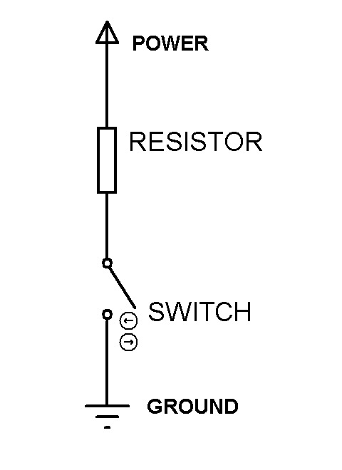
    Now comes the tricky part and unfortunately I can't help you that much. We have to select the dev board properties. If you have purchased it from xilinx odds are you will just have to select it from the Evaluation Development Board menu. If not please check the manual for the info. At Product Category put General Purpose. The device family is easy to find and chances are you have either a Spartan 3 or a Spartan 6. The next two are found in the device manual. For the speed grade I chose the highest value available to me witch is -3. You are free to experiment with it as I didn't find info about it anywhere. The next lines should be exactly like in the picture:


    Click Next and then Finish.
    Now right-click on the name of the project on the upper-left side of the screen and choose New Source:


    Select VHDL Module from the list and give the title andg.


    What we are doing right now is creating the entity from 2 posts ago. So after clicking Next you will be prompted to enter the inputs and outputs.
    You are not obligated to enter those here because they can be manually written in code. 
    For this project let's enter them in the wizard. So we have a and b as inputs and o as an output.


    Click on Next and then Finish. Now our entity is created and the basic VHDL program structure is automatically created.
    The only line you have to enter is: o<=a and b;
    It should go between begin and end Behavioral; and the code should look like this:


    Now it's time to assign the pins through a constraint file. On the left sidebar open the User Constraints tree and select I/O Pin Planing (PlanAhead)-Pre-Synthesis. Right click it and select Run.


    If any question appears after hitting Run select Yes.
    Again here you have to find the pin names for your FPGA and select a LED and 2 slide switches as I showed you in the last post.
    After Plan Ahead opens, in the center of the screen there should be a tree structure like this: All ports -> Scalar ports -> the 3 ports in the entity. Find your pin names and enter them on the Site column like in the picture:


    After that go to File and select Save  Exit PlanAhead.
    The next 3 steps are simple and will not be illustrated. Right-click on Synthesize-XST and select Run. After it is done right click on Implement Design and click Run. Lastly we need to generate a file that programs the FPGA: right-click on Generate Programming File and select Run.
    ISE will generate a file named andg.bit located in the root directory of your project. For me that is: E:\Project ise\test\AndGate. This file contains the code that will program the FPGA's logic blocks and interconnect them if necessary.
    The last part is programming the dev board. If you have a Digilent board then you can use their Adept software. Just plug the device in your PC and select the .bit file. If you are using another board and the drivers for it are installed correctly do the following step to program it with Impact. Open the Configure Target Device tree and right click Manage Configuration Project (iMPACT). Select Run.
    In iMPACT click on File -> New Project and select Yes, then OK. After the software finds your board select the .bit file and click Open. Right click the circuit symbol and select Program.

    Congratulations! You have done your first project.
    I will be uploading a youtube video shortly to show you how it looks on my board.


Friday, October 28, 2011

Link FPGA I/O to entity I/O

    In the last post I showed you how to declare an entity and how to determine the diagram of a circuit from that declaration. Let's consider that we have the architecture written for that entity:
             
                 o<=a and b;


    So o will be the result of input a and input b or a*b. If we were to implement this design in an FPGA the only way to determine if it is correct would be to somehow link those inputs and output to peripherals attached to the FPGA's pins like LEDs and buttons.

    We can do that using a special file called a constraints file. There are two ways to edit constraints:
       - by using the program witch came from the FPGA vendor (ex: Xilinx ISE, Altera Quartus)
       - manually entering the constraints with a text editor

    Before I give you an example of making a constraints file, I will introduce you to the 3 most basic I/O circuits you will use: LEDs, slide switches and push buttons.

    LEDs
    You have probably seen LEDs (Light Emitting Diodes) everywhere. They are small yet bright and come in different colors, but how do they work?

    LEDs, or any diodes, have two elements called anode and cathode and let current flow only in one direction (from the anode to the cathode) so since current flows from positive to negative we can associate the anode with POWER and the cathode with GROUND. By connecting the two sides of an LED to the positive/negative sides of the voltage source, it will light up.

                          
    In the image the LED is properly connected and it will stay lit as long as the power is up. But it's not what we want. We want a way to control when it lights up and when it shuts down. That's why when linked to FPGAs and other electronic devices, LEDs have one of it's components connected to it's respective power source side (anode to POWER and cathode to GROUND) and the other component connected to one of the pins belonging to the device. This way we control the flow of current.
    In most designs the anode is the part connected to the FPGA pin so if we send power (logic 1) to it, the LED lights up and vice versa for logic 0.

    Slide switches
    They are useful if you want to keep something on or off as long as the switch is in the on/off position.

    The picture shows a slide switch connected to a power source:
    The slide switch is an input circuit because it sends a high (1) or low (0) signal to the device it's connected to. The FPGA pin would connect between the resistor and the switch. It means that when it's open, the FPGA receives a high signal because it's linked only to positive (POWER). If the switch is closed then the circuit is complete (POWER-GROUND) and and the FPGA receives a low signal.
    Another way to link a switch is with a resistor placed near ground and the FPGA pin connected between the down side of the switch and the resistor. This means that when the switch is open it sends a low signal and when it's closed it sends a high signal.

    Push buttons
    They have the exact same style of connecting to the FPGA. The only difference is that they send a high/low signal (depending on the connection type) only when pressed.
                                                       

    How it all ties together
    Let's consider an example FPGA witch has 2 switches, 2 buttons and 2 LEDs. Each pin has a name or a code usually composed of letters and numbers. We need that code in order to link it to the proper input/output in the entity. You can find the pin names in your FPGA user manual or schematics.
    In th entity declaration you can see 2 inputs and an output. The outputs is of course an LED. The inputs can be associated with buttons or switches because they are inputs but the reasonable choice is switches. Why? Because we want to maybe have at one time an input low and an input high and keep them that way. If we use buttons then we need to keep one of them pressed as long as we want the low value.
    The example FPGA looks like this:
    
    
    Let's see our entity again:
                 entity andgate is
                    port(
                            a : in std_logic;
                            b : in std_logic;
                            o : out std_logic);
                  end entity andgate;

    As you can see in the picture the pins are named L1 and L2 for the LEDs, SW1 and SW2 for switches and B1 and B2 for buttons. In real FPGAs the codes are not so logical chosen.
    Now it's time to see how a constraint file looks like. We'll connect a to SW1, b to SW2 and o to L1:

                 NET "a" LOC = SW1;
                 NET "b" LOC = SW2;
                 NET "o" LOC = L1;

    As you can see the NET defines our entity I/O and with the LOC keyword we assign it to a real pin on the FPGA.


Wednesday, October 26, 2011

Introduction to VHDL

    In order to use an FPGA, you of course have to program it first to do something. For this task we need a Hardware Description Language or HDL. There are 2 primary HDLs around:
       -VHDL
       -Verilog
    In my tutorials I will be using VHDL. At least for now.

    VHDL compared with programming languages
    If you look at VHDL code you will be tempted to think that it is a computer programming language at first glance.In fact the only things it shares with a standard programming language like C or Pascal are some constructs like loops (for, while) and the general sintax with lines ended in semicolons and blocks encased in begin and end statements.

    The differences between VHDL and programming languages are it's strong point. Firstly it is by nature a concurent language. So if we have 2 or more concurent blocks of code in a program then they will be executed at the same time, as opposed to C statements witch are sequential. For example a VHDL program with these two lines: A<=B; and B<=A; (witch mean A=B,B=A) will execute does instructions concurently. So A and B will swap values. In a C program if we had A=B; and B=A; you would lose A's value.
    Another big difference is that VHDL not only lets you describe circuits, but it has timing constructs that let you simulate them on the computer first.

    The basic structure of a VHDL program
    The minimum components are:

       -Library inclusion: similar to thoes used in programming languages; we need to include libraries in order to use certain functions or data types in a program
       -Entity declaration: this part is important because we define the input and output ports of our circuit and their data types. Based on the entity we can make a diagram of the designed hardware, but we don't know yet the functionality of it. So you can think of entities like black boxes. Example of entity declaration and diagram (ignore the data types because they will be explained in another tutorial):


                     entity andgate is
                     port(
                               a : in std_logic;
                               b : in std_logic;
                               o : out std_logic);
                     end entity andgate;


       -Architecture: the main part of the program where we specify how the circuit works. It includes concurent blocks. The blocks can have sequential instructions inside them.


Tuesday, October 25, 2011

Welcome to FPGA Tutorials

    First of all i would like to welcome you to my blog and thank you for taking the time to read this post. As the title would suggest, this blog's role is to provide tutorials on how to program FPGAs.
    If you already know what an FPGA is or what languages are used to program such circuits than you can skip this post, but if these terms are unfamiliar to you, my advice is that you read this article.
    Notice: Every concept talked about in this post will be fully explained in later tutorials. This is just an introduction to the basic ideas and terminology.
 
    What are FPGAs and why do we need them?
    The letters FPGA stand for Field Programmable Gate Array, complex circuits composed by arrays of logic blocks that can be interconnected through programming. So for example we can program an FPGA to be a sound card or maybe a processor or a custom circuit designed by you.

    The second most important component of an FPGA  is I/O. These chips have I/O pins all around in order to hook up peripherals ranging from LEDs to to different sensors.
    This a very basic structure of a Field Programmable Gate Array:

    As you can see 3 of the logic blocks are connected to each other so that they can perform a more complex task or to form a specific circuit. For example let's consider that we a light sensor and 8 LEDs attached to the I/O pins. Thoes 3 logic blocks could be programmed as a circuit that activates a certain number of LEDs based on the value from the sensor.
    So what makes an FPGA better than a microprocessor or a microcontroller?
    Simple: if for example we have 2 light sensors and 16 LEDs (1 sensor for 8 LEDs) connected to a microcontroller then the operations will be executed one after another (check the first sensor and light up the first 8 LEDs accordingly, and then check the second sensor and light up the other 8 LEDs accordingly). For this case you wold think that it happens instantly but if you had more complex operations maybe the delay between the 2 instructions would be visible.
    If thoes 2 sensors and 16 LEDs would be connected to an FPGA you can program 2 independent circuits that check light levels and activate the LEDs at the same time. So for more complex operations an FPGA wouldn,t have that lag between instructions like the microcontroller.

    FPGA manufacturers
    The two leading companies in the world are
        -XILINX   Site
        -ALTERA   Site

    In my tutorials I will be using a Xilinx Spartan 6 FPGA development board.

    Development boards
    In order to use FPGAs you can't just buy the chip because i doesn't have I/O circuits or programming ports, it just has pins. That's why you need a development board. That is a printed circuit board witch contains the FPGA, I/O circuits (LEDs, switches, push buttons), video out/in ports, communication ports (UART) and other useful circuits for basic to advanced digital design.
    Such a development board looks like this:

    A very well known dev board manufacturer is DIGILENT. You can find information about thier products, prices and helpful documents on thier website: Digilent website